In Single Cycle processor, as its name, it should done one instruction in one clock cycle(which also means CPI=1). But it seems that the latencies varies from instruction to instruction. In order to guaranty every instruction finish, the clock cycle is determined by the longest instruction latency. Yes, that’s wasting lots of time.
Can we have a better solution? We can partition each sub-instruction or(sub-behavior). In this section, we should try to balance the time spend in each section.
For each partition, we need to determine some registers the datapath should be accessed. In other words, we need to store something from previous partition, and use them in current partition.
We can have an example on I-type operation. It can be done in 4 clock cycle.
- IR <- IM[PC]
- A <- R[rs]
- s <- a op zero_ext(imm)
- R[rt] <- S; PC <- PC+4
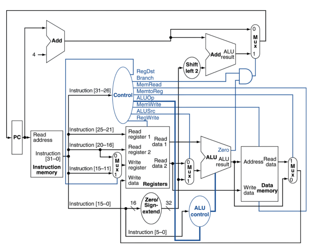
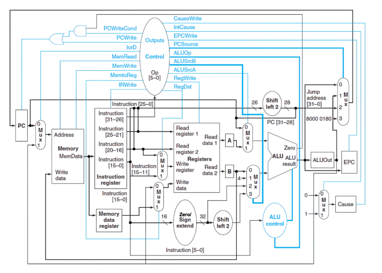
Comparing 2 picture above, we can observe multiCycle Processor has a much complexer control unit(FSM). And some registers are added to design, dividing a Processor to several part. The main reason of FMS has more signal output is the increased number of registers.
However, consider we have are doing an I-type operation. When we are doing A <- R[rs], the previous part(instruction registers) is unused. That’s a kind of resource waste. To solve it we can design a Pipeline processor.